


Texas Instruments SN74LXC2T45/SN74LXC2T45-Q1 Dual-Supply Transceiver
Texas Instruments SN74LXC2T45/SN74LXC2T45-Q1 Dual-Supply Transceiver is a dual-bit, non-inverting bi-directional voltage level translation device. Ax pins and the control pin (DIR) are referenced to VCCA logic levels, and Bx pins are referenced to VCCB logic levels. The Texas Instruments SN74LXC2T45/SN74LXC2T45-Q1 A port can accept I/O voltages ranging from 1.1V to 5.5V, while the B port can accept I/O voltages from 1.1V to 5.5V. A high DIR allows data transmission from A to B, and a low DIR provides data transmission from B to A. The SN74LXC2T45-Q1 devices are AEC-Q100 qualified for automotive applications.
Features
- A fully configurable dual-rail design allows each port to operate from 1.1V to 5.5V
- Robust, glitch-free power supply sequencing
- Up to 420Mbps support for 3.3V to 5.0V
- Schmitt-trigger inputs allow for slow or noisy inputs
- I/O’s with integrated dynamic pull-down resistors help reduce external component count
- Control inputs with integrated static pull-down resistors allow for floating control inputs
- High drive strength (up to 32mA at 5V)
- Low power consumption
- 3µA maximum (25°C)
- 6µA maximum (–40°C to 125°C)
- VCC isolation and VCC disconnect (Ioff-float) feature
- If either VCC supply is < 100mV or disconnected, all I/O’s get pulled down and then become high-impedance
- Ioff supports partial-power-down mode operation
- Compatible with LVC family level shifters
- Control logic (DIR) are referenced to VCCA
- Operating temperature from –40°C to +125°C
- Latch-up performance exceeds 100mA per JESD 78, class II
- ESD protection exceeds JESD 22
- 4000V human-body model
- 1000V charged-device model
Applications
- Eliminate slow or noisy input signals
- Driving indicator LEDs or Buzzers
- Debouncing a mechanical switch
- Infotainment head unit
- ADAS fusion
Datasheets
Functional Block Diagram

Related Development Tools
Texas Instruments 5-8-NL-LOGIC-EVM Logic & Translation EVM
Configured to support DTT, DRY, DPW, DTM, DQE, DQM, DSF, or DTQ logic and translation packages.
Texas Instruments 5-8-LOGIC-EVM Evaluation Module
Developed to support leaded Logic devices in the DBV, DCK, DCT, DCU, and DRL packages.
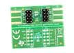
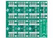
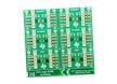
Texas Instruments AXC2T-SMALLPKGEVM Evaluation Module
Configured to support DTM and RSW packages for the AXC and LVC family of bidirectional devices.
Published: 2022-01-26
| Updated: 2022-10-31